
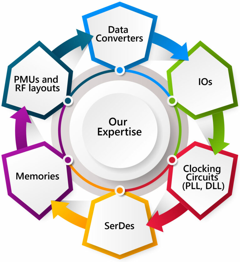
Over the last 20+ years, MosChip has been involved in layouts on many analog and mixed-signal chips. Zapnix Semiconductor has been involved in tape-outs targeted to 14nm/10nm/7nm process nodes. Zapnix Semiconductor team has experience with TSMC, Global, and Samsung Foundries. The Zapnix Semiconductor team has expertise in handling layouts on high-frequency PLLs. The team has expertise in SerDes, PMUs, RF designs, Memories, Data Converters, and IOs.
When it comes to analog circuit creation, we excel in every aspect, encompassing amplification, switching, filtering, conversion, and power provision. Our designs showcase impressive capabilities, enabling high-speed operations that can reach up to an impressive 100 MHz. Moreover, our circuits have remarkably low current requirements, measuring in picoamps, and operate at ultra-low voltage levels in the microvolt range.
One of our core strengths lies in our ability to maintain minimal noise levels and prevent any interference with high-speed digital circuits that may exist on the same board. This expertise ensures that our analog circuits perform flawlessly in any environment, providing accurate and reliable results.

Copyrights 2024©, zapnix. All Rights Reserved.