
Physical Design Services
Zapnix Semiconductor specializes in RTL to GDSII using both Cadence and Synopsys flows. We not only maintain leading EDA infrastructure for physical design, but also employ a team with dedicated subject matter experts with rich experience in the physical design flow and methodologies critical to achieving optimum performance, power, and area (PPA).

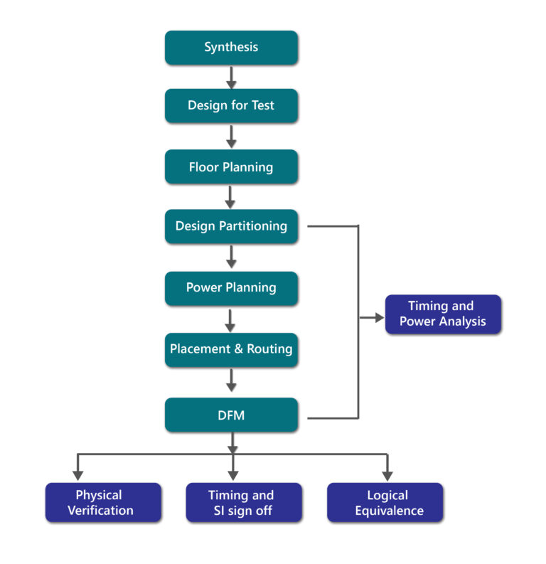
Our key offerings as part of our Physical Design services encompasses the following:
We help our customers make the choice of the foundry for tape-out, which is one of the most critical aspects of the process. Zapnix Semiconductorclosely works with leading foundries including TSMC, GF, etc. Over the last 20+ years, Zapnix Semiconductor has been involved in Synthesis, Physical Design, and Timing Closure on quite a few multi-million gate chips with frequencies running up to 1.2GHZ and with low power intent implemented.
Zapnix Semiconductor been involved in tape-outs targeted to 14nm/10nm/7nm process nodes. Zapnix Semiconductor team has experience with TSMC, Global, and Samsung Foundries. Zapnix Semiconductor has developed synthesis, physical design, and timing flow that has been successfully used on a large number of designs. The team has strong expertise in implementing low-power techniques – Clock Gating, Multi-Vt, Voltage Islands, and Power Gating.

Our Expertise
Copyrights 2024©, zapnix. All Rights Reserved.